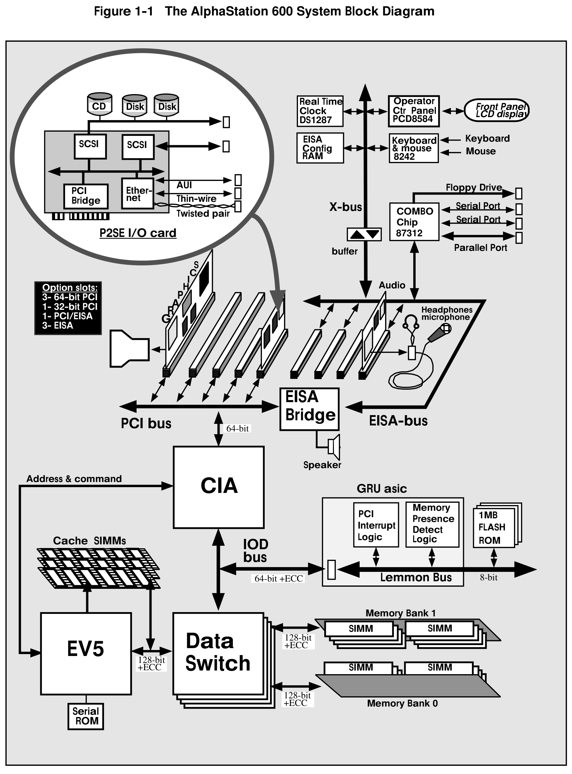
AlphaStation 600 Series Technical Reference Information,
EK-AS800-RM.A01, July 1995
Previously on My side quest: A dead AlphaStation: the Alpha gets stuck somewhere during the DE step of the initialisation sequence. To find out where, we need to obtain the SROM code and try to follow it somehow.
The Alpha’s previous owner, Jonathan, had already dumped and disassembled the full SROM image. I modified his program to pass the -m alpha:ev5 option to objdump, which turns on decoding of PALcode-specific instructions for the 21164 CPU. objdump still does not show internal processor register names in HW_MFPR/HW_MTPR instructions, but Jonathan’s code adds them in post-processing. This was perhaps another opportunity to use Klaus Kämpf’s Ghidra plugin for Alpha, but then again, Ghidra needed installing and setting up and all that.
Here is the disassembly of the main stream 0 code with additional commentary that I made on this journey. (For reference, others are also available: stream 1, stream 2, stream 3, stream 4, stream 5, stream 6, and stream 7). This is what it looks like:
      0:  0f 01 ff 77    hw_mtpr    zero,0x10f          ; ICM
      4:  56 01 ff 77    hw_mtpr    zero,0x156          ; PALtemp22
      8:  57 01 ff 77    hw_mtpr    zero,0x157          ; PALtemp23
      c:  39 00 40 d3    bsr        ra,0xf4             ; DF - init CPU
     ...
Whilst I couldn’t find a Technical Reference Manual for this machine, there was one kicking around for a slightly older model from the same family, the AlphaStation 600 (codename ‘Alcor’). It turned out to be so remarkably similar that I could use this manual for my Alpha (500/500 model, a.k.a. ‘Bret’) with no difficulty.
AlphaStation 600 Series Technical Reference Information,
EK-AS800-RM.A01, July 1995
The processor manual is a useful reference on PALmode programming and Internal Processor Registers, essential for understanding how the SROM code initialises the system.
The CIA is well described in the AlphaStation 600 Technical Reference. Having cross-checked it against the 21172 Core Logic Chipset TRM, I concluded that 21171-CA and 21172-CA appeared to be identical from the programming standpoint.
The Data Switch chips are not directly accessible from software; they are controlled by the CIA.
I couldn’t find any dedicated GRU ASIC documentation. However, both AlphaStations use the same DC7560A chip, and the Technical Reference for the 600 model has got everything we want to know about it.
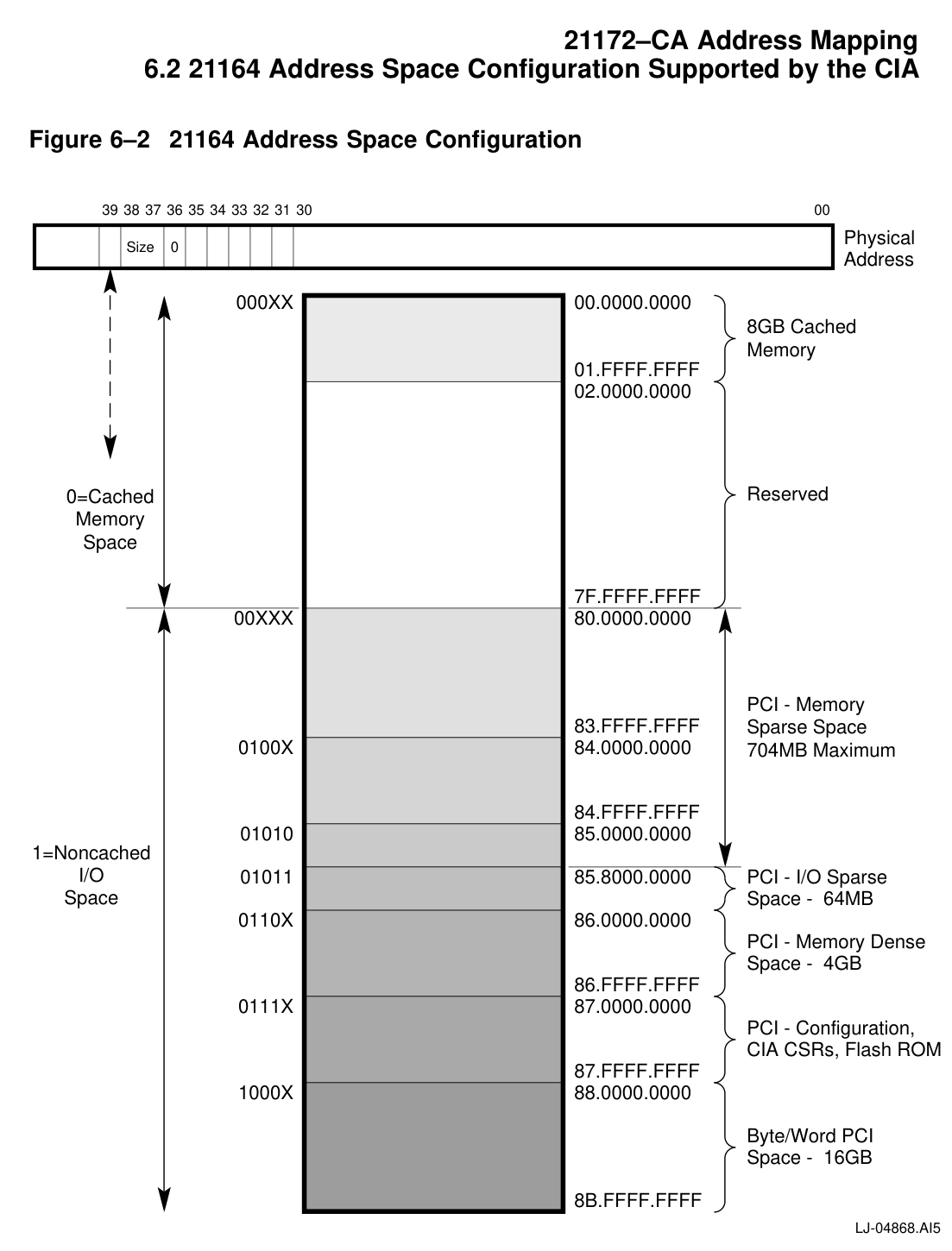
21172 Core Logic Chipset Technical Reference Manual,
EC–QUQJA–TE, 1996
The Alpha initially lacked load and store instructions for bytes and 16-bit words. Although the addresses were byte granular, byte access required multiple instructions to extract or insert bytes whilst using the wider load/store bus transactions.
However, this wouldn’t work for I/O devices that needed true byte addressing on the bus. For that, ‘Sparse’ spaces were provided. Access width in a sparse space is encoded as part of the address. A ‘sparse’ address is essentially an I/O address shifted left by 5 bits, with bits <4:3> filled with the size code (on top of the base of the sparse space). The result is a quadword aligned address for that I/O device register.
The CIA translates sparse accesses on the CPU bus to the appropriately sized PCI bus transactions. It also maps a ‘dense’ address space onto the PCI bus, which is a straightforward 1:1 mapping – but only works with longwords and quadwords (4 or 8 byte units).
Alright, now we are ready to poke some addresses. Let’s begin with the diagnostic LEDs, because we know that they work.
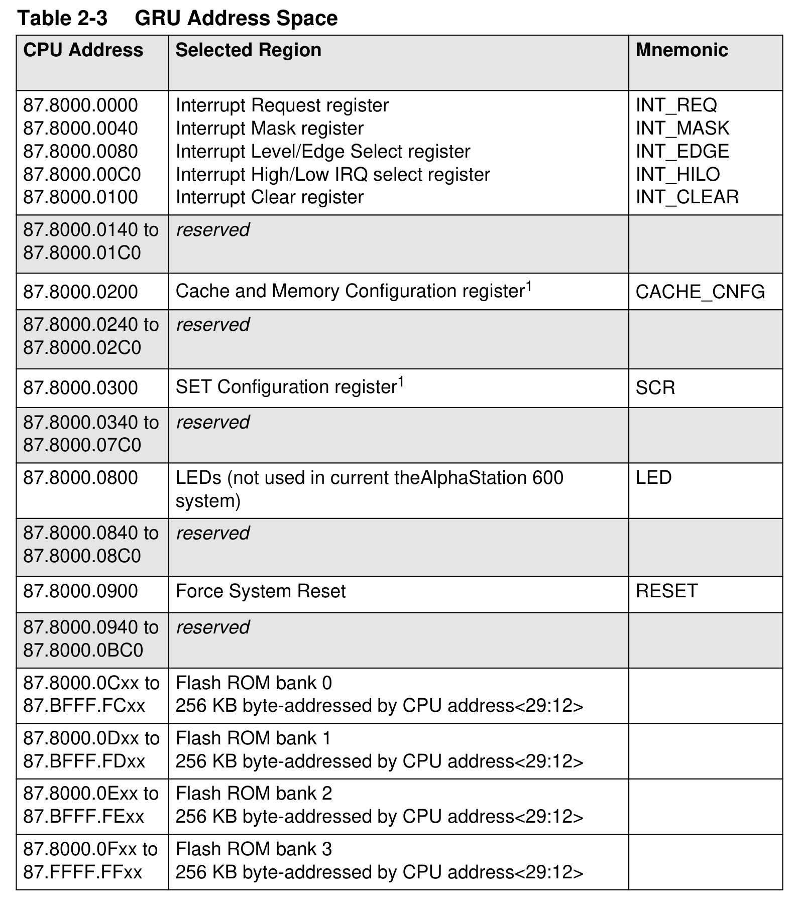
We’ll need these two commands:
As described in the AS600 TR, the LEDs are controlled by bits <7:0> in the write-only GRU register at address 87.8000.0800. I place the jumper onto J19, set the terminal to 19 200 baud, type ‘U’ to start the console, and enter the commands:
Bret SROM V2.05
000001f5 MHz
Console

SROM> ba
AL> 80000800
AH> 87
BaseAddr  ON:   00000087.80000800

SROM> dm
A> 0
D> be

SROM>
‘BE’ shows up on the LED display. Not exceedingly surprising, but a good start anyway.
There is only one button present on the front panel, and it can act as HALT or RESET as determined by jumper J6. I placed the jumper onto pins 1 and 2 for RESET and pressed the button, but nothing happened. Even after cleaning up the pins and having tried different jumper positions, I still couldn’t get the button to reset the machine.
Okay, let’s try the software approach.
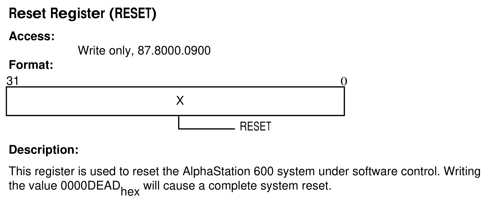
The RESET register is located at offset 0x100 from my previously set BaseAddr. I follow the instructions in the description, and the system promptly restarts.
SROM> dm
A> 100
D> dead
Good; I’m going to need a lot of restarts to investigate where the start-up goes pear shaped, and I don’t want to power cycle the machine each time.
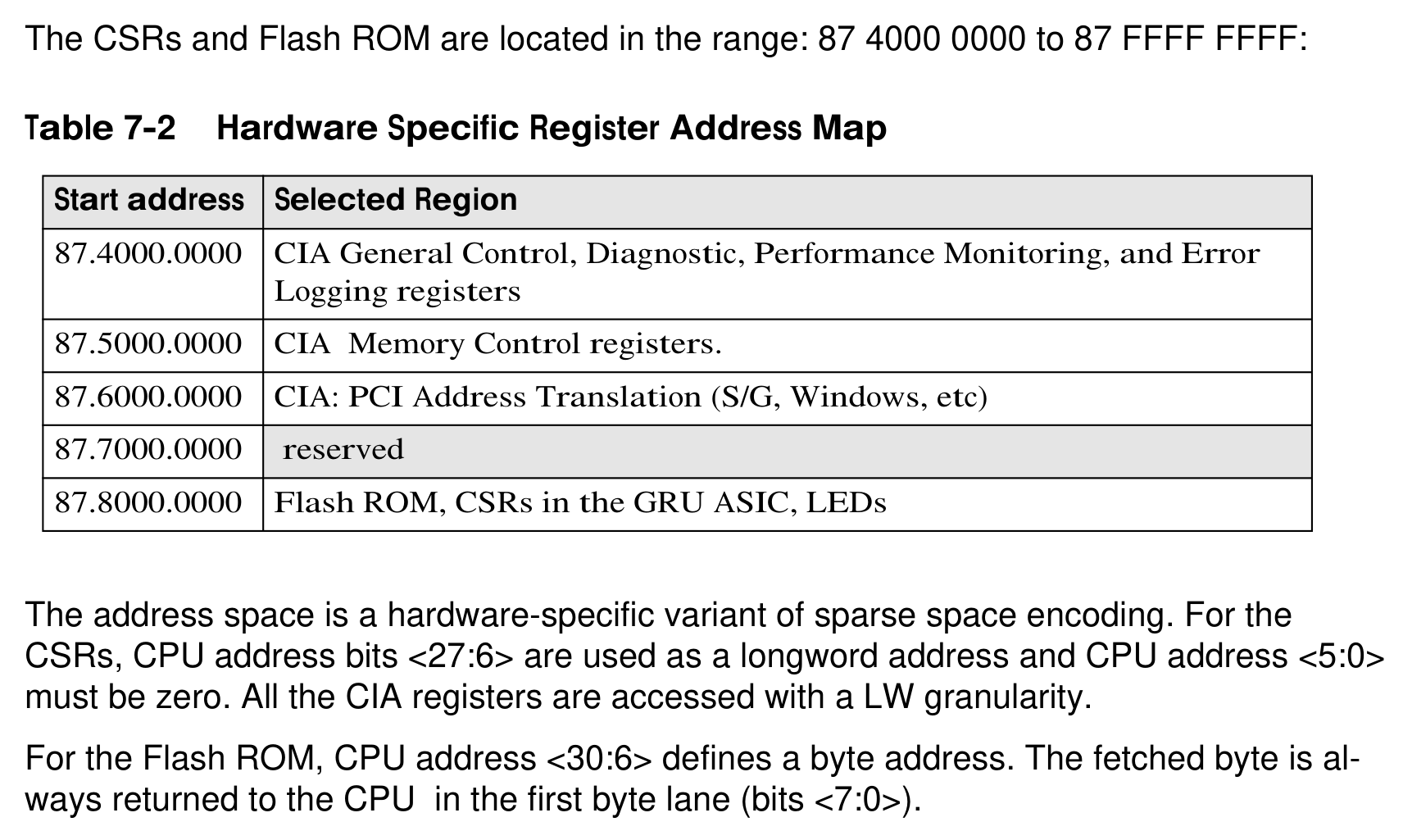
Here’s what I got; the comments are mine, based on the 21172 TRM.
87.40000080: CIA_REV      00000002  <8>=0 — High-asserted ras and cas; <7:0>=2 — Pass 3 CIA chip present.
87.40000100: CIA_CTRL     80004000  defaults except CON_IDLE_BC=1
87.40000140: CIA_CNFG     00000000  defaults
87.40000480: CFG          00000000  defaults
87.40002000: CIA_DIAG     00000000  defaults
87.40003000: DIAG_CHECK   000000b2  ok, <7:0>=undefined
87.40008000: CPU_ERR0     fffffff0  ok, latches error address
87.40008040: CPU_ERR1     002010ff  ok, <31> CPU_PE=0 - CIA has not logged a system bus error.
87.40008200: CIA_ERR      00000000  ok, <31> ERR_VALID=0 - An error has not been detected.
87.40008240: CIA_STAT     00000018  hmm, <03> MEM_SOURCE=1—PCI is the source of the memory cycle.
Everything is as it should be after power-up, except for one suspicious bit in CIA_CTRL and one in CIA_STAT.
The next step is to take a look at the SROM disassembly and follow the initialisation sequence in the mini-console to see how far we can get.
The LED display routine (which I call diag_leds in my annotations) is located at
address 179c and takes register t11 as input. At address
158, it is invoked with the DE sequence code, after which the program proceeds to load
and read back a bunch of registers. I follow along.
Bret SROM V2.05
000001f5 MHz
Console

SROM> ba
AL> 60000000
AH> 87
BaseAddr  ON:   00000087.60000000

SROM> em
A> 400
00000087.60000400: 74c00004

SROM> dm
A> 400
D> 0

SROM> em
A> 400
00000087.60000400: 00000000

...
etc. (see full transcript here).
Everything reads back correctly.
Earlier, during normal power-up, I tried monitoring RAM signals (RAS and CAS) and Dallas DS1287 RTC pins – CS, AS, and DS. They were all absolutely lifeless except CS – the active low chip select signal (yellow C1 trace on the oscilloscope), – which went high together with the 5V supply (green C2) and was then driven low some 235 ms later.
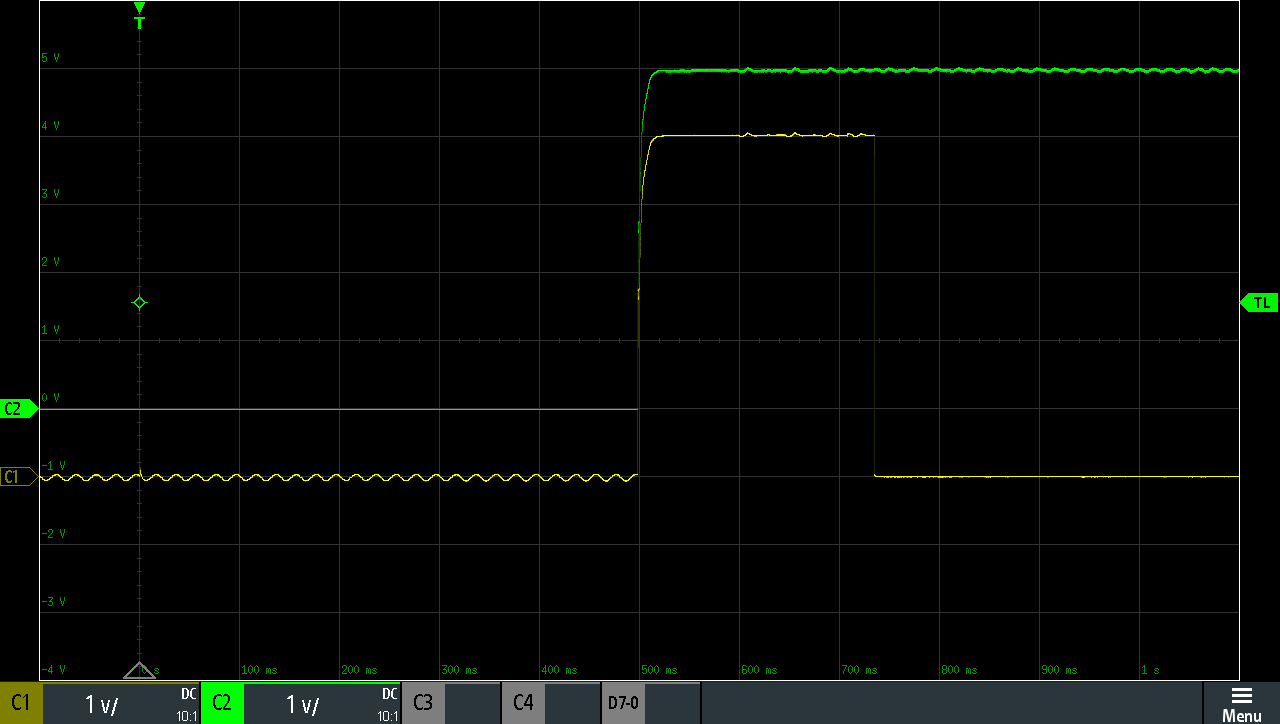
It turns out that, during manual CIA initialisation in the no-init console, CS stays high until
a104e0f3 is deposited at address 87.4000.0100 – into the CIA_CTRL register. This write
sets bit <0>, PCI_EN, to 1, instructing the CIA to deassert reset of the PCI bus. In all
likelihood, this is what activates CS on the Dallas RTC, driving it low.
The Intel 82374SB EISA System Component (ESC) chip only engages the DS1287 control signals (AS, DS, R/W) when the RTC is being addressed, and therefore does not need to operate Chip Select. In fact, the ESC does not even have a designated CS output for the RTC. I checked continuity from the Dallas CS on the main board and tracked it down to pin 111 of the ESC chip. That is the general purpose RSTDRV output, which is indeed a simple inversion of the PCI reset signal.

Having completed CIA initialisation, the SROM code at 1e8 calls subroutine
1e3c, where it ventures further out, onto the PCI bus. The manual process has so far
shown no obvious anomalies, but pressing ahead with it is going to get tedious, slow, and
error-prone. I need to find a way to modify the SROM code and load it into the Alpha CPU’s
instruction cache. I don’t have a UVPROM programmer. Even if I did, plugging and unplugging the
ROM all the time would ruin the freedom of iteration. I wonder whether my Raspberry Pi Pico 2W can
help me here.